Mehrdad Rostami Osanloo
Research Scientist | Semiconductor Industry
Research Scientist at Tokyo Electron US, bridging atomic-scale physics, process engineering, and device integration in the semiconductor industry.

Research Scientist, TEL
Research Scientist at Tokyo Electron US, bridging atomic-scale physics, process engineering, and device integration in the semiconductor industry.
Research Scientist, TEL
Research Scientist / Quantum Chemist
Tokyo Electron US (2022 – Present)
Developing predictive, physics-based models for next-generation semiconductor processes, supporting advanced logic and memory nodes.
Supporting the transition to sub-3 nm nodes through atomically precise material removal, improved selectivity, and defect control for nanosheet GAA transistors and 3D integration.
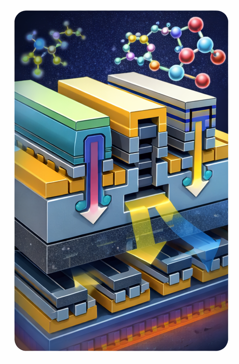
Atomically controlled thermal etch strategies for nanosheet gate-all-around architectures, enabling uniform sheet release and tight CD control for sub-3 nm logic nodes.

Investigation of cryogenic plasma etch regimes for highly anisotropic profiles in extreme high-aspect-ratio structures for advanced 3D device integration.
Physics-driven exploration of etch chemistries combining first-principles modeling and kinetics analysis for next-generation etch processes.
The University of Texas at Dallas (2019 – 2022)
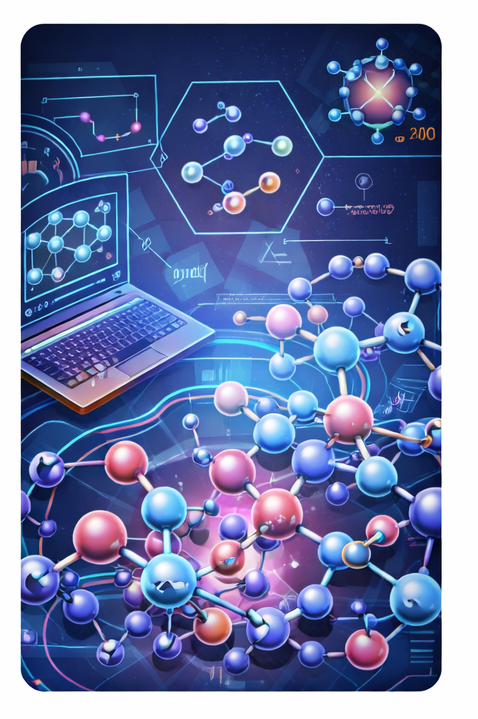
I explored 2D van der Waals dielectrics as alternatives to traditional materials, identifying promising candidates for low-power, next-generation transistors through advanced first-principles calculations.

Open to research collaborations, invited talks, and technical discussions related to computational materials science, plasma processing, and semiconductor manufacturing.